STUDY
MATERIAL
COURSE: M.Sc Software Systems
Semester:
I
SUBJECT: APPLIED PHYSICS
UNIT : IV
Staff: K. SUBRAMANIAN
SYLLABUS
UNIT
I
Lasers and fibre optics:
Construction and working of He-new laser - co2 Laser Ruby laser -
Semi conductor laser - Application.
Types of optical fibre - singled and bundled fibres - Fbre
material - Attenuation -
Dispersion - Fibre optic light sources - Detectors - Fibre optic
communication - Principles
of optical recording.
UNIT II
Super conductor: Qualitative
study of the phenomenon - Critical temperature and critical
field. Meissner affect -
Josephson Effect - Type I and type 2 super conductors. BCS theory of
super conductivity
(Qualitative) - high temperature super Conductors.
- Application: Cryotron.
Magnetic leviation -Super conducting magnets.
UNIT III
Electrical properties: Free
electron theory of drude and Lorentz - weidmann- Franz law -
Distinction between
conductors, Semi conductors and insulators on the basic of band theory -
Factors affecting the
resistivity of a conductor:
Temperature, Alloying,
Pressure, Strain, Magnetic field and environment.
UNIT IV
Semi conducting materials:
Intrinsic, Extrinsic semiconductors - Material preparation:
Czochralski method - Zone
refining. Hall Effect in semi conductor - applications. Physics of
PN junction diode - Junction
transistor. Dielectrics :
Permittivity - Dielectric
constant - Dielectric polarization - - Types of polarization - Break
down mechanisms.
UNIT V
Magnetic properties : Ferro
magnetism: Dornine theory - Hysteresis - Hard and soft magnetic
materials - Curie - - Weiss
law - Magnetossniction. Ferrites : Preparation, Properties,
Applications - Magnetic
bubble memory.
REFERENCE BOOKS:
1. Brijal and Subramanian,
“Optics”, Chand and co 1995.
2. V. Raghvan, “Material
science and engineering”, a first course, prentice hail of India 1991.
3. M.R. Srinivasan, ‘Physics
for engineers’’, New age international pvt ltd publications,
1996.
4. Seth and Gupta, “Course
in electrical engineering materi3ls”, Dhanpat Rai and Sons, 1990.
5. M. Arumugam, “Material science”, new age
international pvt ltd publications, 1996.
UNIT I
LASER AND FIBER OPTICS
LASERS
Laser is an acronym for light amplification
by stimulated emission of radiation.
Lasers are basically optical sources that produce light radiations with
high degree of intensity and coherence (monochromaticity and directionality)
Each of these characteristics that are not normally
found in ordinary light makes laser a unique & the most powerful tool. Lasers find a wide variety of applications in
the field of scientific research, engineering & medicine.
According to Einstein the interaction of radiation with
certain matter involves three basic
processes:
· · Excited
atoms · · · · ·
Incident photons ÙÙÙ> ÙÙÙ> emitted photon
ÙÙÙ> Incident
photon
Stimulated absorption spontaneous emission stimulated emission
Stimulated absorption: When an electromagnetic radiation of
frequency n is incident on a sample of
atoms, the electrons in the lower energy state (E1) absorb the
energy from the incident radiation & rise to the higher energy state (E2). This process is called stimulated absorption.
Spontaneous emission: The atoms excited to higher
energy state are unstable there. Their life time t in these states is of the
order of 10-8s. The electrons in these
states spontaneously make transition to lower energy states emitting a photon
whose energy hg is the difference between
the two energy states E2 and E1 i.e, E2-E1
This type of transition of an electron
from a higher to a lower energy state without any outside stimulus is
called spontaneous emission. The photons so emitted are in random phases
and random directions.
Stimulated emission: When a photon of energy hn = E2-E1 is incident on an atom which is
already in an excited stateE2, the atom being disturbed or
stimulated by the incident photon, makes a transition to a lower energy state E1
emitting a photon. The emitted
photon has the same frequency, phase & direction as the incident
photon. This type of emission is called stimulated
emission. The net effect is two identical photons in the place of one
thereby increasing the intensity of the incident beam. It is this process of stimulated emission
that makes possible the amplification of light in lasers.
Metastable
Energy Level
Metastable states: The time interval that corresponds to 0.5
probability of transition of atoms from the excited state is called the half
life of the excited state. In the
visible region, the half-life of an atomic transition is 10-8 s.
Those energy states, where the atomic transitions
have a much longer half life (10-3 s) are called metastable
states. Existence of metastable
state is necessary for achieving population Inversion.

(Fig. 4)

An electron
excited to level A will stay much longer (say 10-4 sec) compared to a
“normal” energy level where an electron typically stays for 10-8 sec
(provided there is no external
perturbation, stimulated emission can occur immediately).
IV. Population
Inversion
Consider some
atoms (or molecules) in space as shown in the diagram below.

(Fig. 5)
When there are
more atoms with an electron in level A, we say that there is population
inversion.
Essential components of a laser
The laser device basically consists of three elements.
1. A pump
2. An active medium
3. A cavity resonator or an optical cavity.
Pump: is an
external energy source that pumps sufficiently high energy to excite the atoms
/ molecules to higher energy states & produce population inversion a
necessary condition for stimulated emission. Pumps can be optical, electrical,
chemical or thermal.
(i) Optical
pumping: uses light energy for excitation. This is the only practical
method of pumping the atoms in solid & liquid laser medium. Eg. Ruby laser uses xenon flash lamp.
(ii)
Electrical discharge: a) Collision of First kind
(electron-atom collision). When a current of electrons is passed through the
lasing gas medium, the conduction electrons collide with a large number of
atoms, ions or molecules & raise them to the excited states.e+x "x*+e. Such a process is called a collision of First
kind. This method is preferred in gaseous lasers which contain one gas
species. Argon laser uses this
technique.
(b) Collision of second kind (Inelastic atom-atom
collision): In some lasers, the laser atoms are directly excited to the desired
states by means of inelastic collisions between the atoms or molecules.
A mixture of two different gas species of atoms A
& B is used in which the excited energy states of A* & B*
coincide. Energy may be
transferred from the excited state of (say)
A to the other B through inelastic collision between A* & B symbolically
represented as
A* + B ® A + B*-DE. This method of transfer of energy is called resonant
transfer or collision of second kind.. Helium-neon laser, CO2
are notable examples using this technique of pumping.
(iii) In semiconductor lasers the electrical energy
is used to pump electron from valence band to conduction band.
(iv)
Chemical reaction in certain materials leaves the atoms in the excited states.
Eg. dye lasers
2. Active medium: An active medium is a lasing medium which may be a solid, or a liquid
or a gas with atleast 3 energy levels as follows.
a) a ground state Eg
b) a high energy pump state EP
in which the excited electrons remain for only a short period (~10 ns)
c) an intermediate level E1 in which the excited
electrons remain for a relatively longer time (~ms). Such energy states with
relatively long life time are called metastable states.
 high
energy state EP
high
energy state EP
pumping
Metastable state E1
lasing
transition
ground
state Eg
The most important requirement of an active medium
is to support population inversion between two energy levels involved in lasing
transition.
For achieving population inversion, the energy
absorption must occur for a transition different from the transition undergoing
stimulated emission. This shows that,
atleast a 3-level system is required for lasing action.
Generally the lasers are
named after the lasing medium used. For
example, ruby laser, He-Ne laser, CO2 laser, Nd-YAG laser, argon
laser and so on.
It is the active medium that decides the wavelength
of the laser emitted.
Laser action has been observed in over half of the
elements known, with the range of available wavelengths extending from
ultraviolet to infrared region. Gases as
active medium alone give rise to more than 1000 transitions. Two of the mostly
used transitions in gases are 632.8nm visible radiation from neon & 10.6 mm infrared radiation from CO2
molecule.
Though
the active medium should have atleast 3 energy levels there are active media
with 4-levels
In a 3-level laser, the lasing transition terminates
at the ground state. At least one half of the ground state atoms will have to
be pumped to the higher state in order to start the lasing action. Therefore it requires high pumping power. Generally 3-level lasers operate in pulsed
mode.
In
a 4-level system there is a fourth level E2 above the ground state.
The laser transition does not terminate at the ground state but terminates at E2.
Since E2 decays fast into the ground state, the population inversion
can be maintained continuously between E1 & E2.
Moderate pumping is sufficient to maintain this. Generally A
4-level lasers operate in continuous mode.
 EP Pump
state EP
EP Pump
state EP
non radiative transition
E3 metastable state E1
Lasing transition
E2
fast decaying level E2
non
radiative
E1
ground state Eg
In same lasers the
amplifying medium consists of two parts, the laser host medium and the laser
atoms. For example hos of the Nd: YAG
laser is a crystal of yittrium, aluminium, garnet (Commonly called YAG) laser
is a crystal of atoms are the trivalent neodymium ions. In gas lasers consisting of mixture of gases,
the distinction between host and laser atoms is generally not made. In ruby laser Al2O3 is
hot molecule while Cr+3 ions are lasing ions.
Cavity resonator: is an optical feedback
device that directs the photons back & forth through the active medium so
as to maintain saturation intensity within the medium.
|
|||||
reflector ·· partial reflector
The back and forth reflections at the two optically
plane mirrors, placed parallel to each other at the two ends of the laser tube,
make the emitted photons travel through the active medium several times. Those excited atoms that are not triggered
first time are triggered in the subsequent passage. This ensures that all the excited atoms of the active medium participate in the
stimulated emission enhancing the
lasing action. Further, resonance
occurs for those waves that exactly fit into the length L of the laser
tube. i.e., the tube length is such
that L=nl/2where n is a integral
number known as longitudinal mode number.
For a given length L of the tube more than one wave length will fit into
the tube and laser is called multimodal. The absorption of energy being maximum
under resonance condition, laser beam of maximum amplitude is produced.
Types of lasers
Based on the active medium being solid, liquid or
gas, lasers are classified as solid laser, liquid lasers and gas lasers. Based on the gain of the medium lasers are
classified as low density gain and high density gain lasers based on kind of output,
lasers are classified as pulsed or continuous wave (CW) lasers.
Examples :
(i)
Ruby laser, solid
high gain pulsed laser
(ii)
Neodymium laser,
solid high gain operating in continuous wave mode (CW)
(iii)
Semiconductor
lasers, solid state, high gain.
(iv)
Dye lasers: liquid
high gain, operates both in pulsed and continuous wave.
[Note:In contrast to solid lasers the liquid lasers
do not crack or shatter. They can be made in unlimited sizes]
(v)
Helium neon laser
an atomic gas laser, low gain CW mode continuous or pulsed mode is an ion
laser.
(vi)
Carbon dioxide
laser molecular gas lowgain, CW mode power>200kW emitting at 10.6 μm is an
example.
(vii)
Excimer laser:-
noble gas halides, (XeF, KrF, ArF) low gain, pulsed.
(viii) Argon ion – gaseous, low gain, CW.
Ruby Laser
Ruby is a crystal of
aluminium oxide (Al2 O3) doped with chromium oxide (Cr2
O3) in 0.05% concentration. Al & O2 are inert
atoms & chromium is the active medium
Construction
ruby rod helical flash lamp
 Highly polished mirror
C C C
C C partially
silvered mirror
Highly polished mirror
C C C
C C partially
silvered mirror
· ·
pulsed high voltage
It consists of a cylindrical rod of ruby a few mm in
diameter & a few cm in length with its ends perfectly flat & parallel
to each other. One end is highly
polished to act as mirror, while the other end is partially silvered to make it
partially transmitting to get the laser out put. The crystal is surrounded by a flash lamp
connected to a pulsed high voltage source. The flash lamp is a helical quartz
tube with xenon enclosed in it. The rod
is protected from the heat produced by the intense pulse each time, through a
cold-water circulation system.
Working
3 level energy system of
chromium in ruby crystal
 Pumping state EP
non radiative transition
pumping 694.3 nm
E1 metastable sate
Lasing
transition
An
intense flash of light from the flash lamp excites a large number of chromium
ions into the energy state EP. Some of the excited electrons make
transition to the intermediate metastable state E1, through
non-radiative transition. The energy released as heat in this process will be
dissipated into the lattice. A large population of electrons accumulates in
this level resulting in population inversion between Eg &
E1.
The
first chromium ion that makes a spontaneous downward transition to from E1to
Eg radiates a photon that triggers the other excited chromium atoms
in F1 resulting in lasing action.
The ruby laser emerges as a pulse, lasting as long as the excited atoms
remain available in the metastable state. When the excited atoms become
depleted, the lasing action ends & has to be started again by another flash.
The back
& forth reflections at the end surfaces make the photon travel through the
ruby rod several times. The excited chromium atoms that were not triggered
first time are triggered in the subsequent passage of the photon. This ensures that almost all the excited
chromium atoms participate in the stimulated emission enhancing the lasing
action. The ruby rod acts as a resonant cavity for those waves that exactly fit
into the length of the rod L integral number of time half a wavelength. (L=nl/2)
Since the ruby laser is a 3 level laser, the lasing transition terminates
at the ground state resulting in a pulsed output.
Helium-Neon Laser
The
helium–neon laser is an example of the 4-level gas laser that produces a
continuous output of laser. The active medium is the neon. The helium atoms
serve as a pumping medium.
Power supply Quartz tube

Partially silvered mirror
Fully silvered
mirror
Electrodes
polarised
laser
beam
Brewster’s
window
Construction:
It
consists of a glass or a quartz discharge tube about 1 cm in diameter & 0.5
m in length filled with helium at 1mm pressure & neon at 0.1mm
pressure. The tube windows are set at
Brewster’s angle to allow only the linearly polarized light parallel to the
plane of incidence to participate in
stimulated emission & to reflect away from the
cavity those components of light oscillating perpendicular to the plane of
incidence. Two optically plane mirrors
are placed at the two ends. One mirror
is fully silvered to reflect 100 % light while the other is partially silvered
( 95% reflectivity) to make it slightly
transmitting.
Working
A source of high voltage (~1kV) across the
electrodes sends a current of electrons through the tube. These electrons collide with the helium atoms
as they are present in large number
& excite them to the 2s level.
Since the 2s level in helium is a metastable state, the excited atoms
remain there for a long time. The 5s
level in neon has almost the same energy as the 2s level in helium.
Energy
level diagram
 2S
20.66eV 20.61eV
2S
20.66eV 20.61eV
5S
laser transition
632.8 nm
3p
spontaneous transition
3s
spontaneous transition
1S ground state
2p
Helium
Neon
Under such a condition, the
helium atoms in the excited state transfer their energy to the neon atoms in
the ground state by a process called resonant transfer of energy. This transfer of energy will excite the neon
atoms to the 5s state & de excite the helium atoms back to the ground
state.
This can be symbolically
represented as
An
inverted population occurs at the 5s metastable state relative to the 3p state
of neon. An occasionally emitted photon
from 5s level causes stimulated emission of other atoms. The mirrors at the two
ends help in building up an intense coherent beam as the light bounces back
& forth repeatedly.
The stimulated transition from 5s to 3p level
results in a laser beam of wavelength 632.8 nm. There are other transitions
that give rise to laser beam in IR region.
Eventually the atoms from the 3p level come down to the ground state 2p
through an intermediate state 3s by a quick spontaneous transition. This maintains the population inversion
between the 5s & 3p levels providing a continuous supply of laser. If the
length of the discharge tube is adjusted to be equal to n l/2, laser beam of maximum
amplitude is produced.
Though the helium atoms are present in greater
number than the active atoms neon, they do not take part directly in laser
transition. The fairly light helium
atoms can be easily pumped up to their excited states. Without them it is not
possible to directly excite neon atoms so efficiently to the required energy
state.
Applications of Laser: The applications of laser are based on their special properties such as high intensity, directionality & monochromaticity .
Scientific:
1.
Used in investigating the basic laws of interaction of
atoms & molecules with electromagnetic wave of high intensity.
2.
Used as source of monochromatic & coherent beam in
the study of interference.
3.
Measurement of distances & velocity of mobile
objects to a high degree of accuracy.
4.
Used as sources of light in optical fibers
Engineering: Due to its high intensity &
directionality laser is used for
1. drilling fine holes with precision.
2.
accurate welding of fine wires.
3.
cutting & shaping the materials including diamonds
with ease & efficiency.
4.
cutting & sealing of ampules, nipples of feeding
bottles. used in holography, printing.
Holography is a
technique of recording the amplitude & the phase of the light reflected
from objects. This helps in storing the
3-D information.
Medical applications : Laser is used in medicine
as diagnostic & therapeutic instrument. Laser can cut, rupture, open,
vapourise, weld, seal, cauterize, coagulate& heal human tissue. It is the most advanced surgical tool.
UNIT II
SUPERCONDUCTOR
The
Meissner effect
The second defining
characteristic of a superconducting material is much less obvious than its zero
electrical resistance. It was over 20 years after the discovery of
superconductivity that Meissner and Ochsenfeld published a paper describing
this second characteristic. They discovered that when a magnetic field is
applied to a sample of tin, say, in the superconducting state, the applied
field is excluded, so that B = 0 throughout its interior.
This property of the superconducting state is known as the Meissner
effect.The exclusion of the magnetic field from a superconductor takes place regardless of whether the sample becomes superconducting before or after the external magnetic field is applied. In the steady state, the external magnetic field is cancelled in the interior of the superconductor by opposing magnetic fields produced by a steady screening current that flows on the surface of the superconductor.
It is important to recognise that the exclusion of the magnetic field from inside a superconductor cannot be predicted by applying Maxwell's equations to a material that has zero electrical resistance. We shall refer to a material that has zero resistance but does not exhibit the Meissner effect as a perfect conductor, and we shall show that a superconductor has additional properties besides those that can be predicted from its zero resistance.
 Consider first the behaviour of a perfect
conductor. We showed in the previous subsection that the flux enclosed by a
continuous path through zero resistance material – a perfect conductor –
remains constant, and this must be true for any path within the
material, whatever its size or orientation. This means that the magnetic field
throughout the material must remain constant, that is, ∂B/∂t = 0.
The consequences of this are shown in Figure 10 parts (a) and (b).
Consider first the behaviour of a perfect
conductor. We showed in the previous subsection that the flux enclosed by a
continuous path through zero resistance material – a perfect conductor –
remains constant, and this must be true for any path within the
material, whatever its size or orientation. This means that the magnetic field
throughout the material must remain constant, that is, ∂B/∂t = 0.
The consequences of this are shown in Figure 10 parts (a) and (b).In part (a) of this figure, a perfect conductor is cooled in zero magnetic field to below the temperature at which its resistance becomes zero. When a magnetic field is applied, screening currents are induced in the surface to maintain the field at zero within the material, and when the field is removed, the field within the material stays at zero. In contrast, part (b) shows that cooling a perfect conductor to below its critical temperature in a uniform magnetic field leads to a situation where the uniform field is maintained within the material. If the applied field is then removed, the field within the conductor remains uniform, and continuity of magnetic field lines means there is a field in the region around the perfect conductor. Clearly, the magnetisation state of the perfect conductor depends not just on temperature and magnetic field, but also on the previous history of the material.
Contrast this with the behaviour of a superconductor, shown in Figure 10 parts (c) and (d). Whether a material is cooled below its superconducting critical temperature in zero field, (c), or in a finite field, (d), the magnetic field within a superconducting material is always zero. The magnetic field is always expelled from a superconductor. This is achieved spontaneously by producing currents on the surface of the superconductor. The direction of the currents is such as to create a magnetic field that exactly cancels the applied field in the superconductor. It is this active exclusion of magnetic field – the Meissner effect – that distinguishes a superconductor from a perfect conductor, a material that merely has zero resistance. Thus we can regard zero resistance and zero magnetic field as the two key characteristics of superconductivity.
Perfect
diamagnetism
Diamagnetism is due to currents
induced in atomic orbitals by an applied magnetic field. The induced currents
produce a magnetisation within the diamagnetic material that opposes the
applied field, and the magnetisation disappears when the applied field is
removed. However, this effect is very small: the magnetisation generally
reduces the applied field by less than one part in 105 within the material. In diamagnetic
material, B = μμ0H, with the relative
permeability μ slightly less than unity.Superconductors take the diamagnetic effect to the extreme, since in a superconductor the field B is zero – the field is completely screened from the interior of the material. Thus the relative permeability of a superconductor is zero.
2.4
Critical magnetic field
An important characteristic of a
superconductor is that its normal resistance is restored if a sufficiently
large magnetic field is applied. The nature of this transition to the normal
state depends on the shape of the superconductor and the orientation of the
magnetic field, and it is also different for pure elements and for alloys. In
this subsection we describe the behaviour in the simplest situation; we shall
discuss other more complex behaviour in Section 4.If an increasing magnetic field is applied parallel to a long thin cylinder of tin at a constant temperature below the critical temperature, then the cylinder will make a transition from the superconducting state to the normal state when the field reaches a well-defined strength. This field at which the superconductivity is destroyed is known as the critical magnetic field strength, Bc. If the field is reduced, with the temperature held constant, the tin cylinder returns to the superconducting state at the same critical field strength Bc.
Experiments indicate that the critical magnetic field strength depends on temperature, and the form of this temperature dependence is shown in Figure 11 for several elements. At very low temperatures, the critical field strength is essentially independent of temperature, but as the temperature increases, the critical field strength drops, and becomes zero at the critical temperature. At temperatures just below the critical temperature it requires only a very small magnetic field to destroy the superconductivity.
The discovery
of superconductors
The phenomenon of superconductivity, in which the
electrical resistance of certain materials completely vanishes at low
temperatures, is one of the most interesting and sophisticated in condensed
matter physics. It was first discovered by the Dutch physicist Heike Kamerlingh
Onnes, who was the first to liquefy helium (which boils at 4.2 Kelvin at
standard pressure). In 1911 Kamerlingh Onnes and one of his assistants
discovered the phenomenon of superconductivity while studying the resistance of
metals at low temperatures. They studied mercury because very pure samples
could easily be prepared by distillation.
The historic measurement of superconductivity in
mercury is shown in Figure 1. As in many other metals, the electrical resistance
of mercury decreased steadily upon cooling, but dropped suddenly at 4.2 K, and
became undetectably small. Soon after this discovery, many other elemental
metals were found to exhibit zero resistance when their temperatures were
lowered below a certain characteristic temperature of the material, called the critical temperature, Tc,
some of which are given in Figure 2.


The discovery of superconductors
The phenomenon of superconductivity, in which the
electrical resistance of certain materials completely vanishes at low
temperatures, is one of the most interesting and sophisticated in condensed
matter physics. It was first discovered by the Dutch physicist Heike Kamerlingh
Onnes, who was the first to liquefy helium (which boils at 4.2 Kelvin at
standard pressure). In 1911 Kamerlingh Onnes and one of his assistants
discovered the phenomenon of superconductivity while studying the resistance of
metals at low temperatures. They studied mercury because very pure samples
could easily be prepared by distillation.
The historic measurement of superconductivity in
mercury is shown in Figure 1. As in many other metals, the electrical resistance
of mercury decreased steadily upon cooling, but dropped suddenly at 4.2 K, and
became undetectably small. Soon after this discovery, many other elemental
metals were found to exhibit zero resistance when their temperatures were
lowered below a certain characteristic temperature of the material, called the critical temperature, Tc,
some of which are given in Figure 2.

Type I and II superconductors
High
magnetic fields destroy superconductivity and restore the normal conducting
state. Depending on the character of this transition, we may distinguish
between type I and II superconductors. The graph shown in Figure 4 illustrates
the internal magnetic field strength, Bi, with increasing applied
magnetic field. It is found that the internal field is zero (as expected from
the Meissner effect) until a critical magnetic field, Bc, is reached
where a sudden transition to the normal state occurs. This results in the
penetration of the applied field into the interior. Superconductors that
undergo this abrupt transition to the normal state above a critical magnetic
field are known as type I
superconductors. Most of the pure elements in Figure 2 tend to be type I
superconductors. Type II superconductors,
on the other hand, respond differently to an applied magnetic field, as shown
in Figure 5. An increasing field from zero results in two critical fields, Bc1
and Bc2. At Bc1
the applied field begins to penetrate the interior of the superconductor.
However, the superconductivity is maintained at this point. The
superconductivity vanishes above the second critical field, Bc2.
Note that there is superconductivity for an applied field in between the two
critical fields despite the increasing internal magnetic field strength, and
thus the loss of the Meissner effect.


Type
II superconductors are the most useful because the second critical field can be
quite high, enabling high field electromagnets to be made out of
superconducting wire. Most compounds shown in Figure 2 are type-II
superconductors. Wires made from say niobium-tin (Nb3Sn) have a Bc2
as high as 24.5 Tesla – in practice it is lower. This makes them useful for
applications requiring high magnetic fields, such as Magnetic Resonance Imaging
(MRI ) machines. The advantage of
using superconducting electromagnets is that the current only has to be applied
once to the wires, which are then formed into a closed loop and allow the
current (and field) to persist indefinitely – as long as the superconductor
stays below the critical temperature. That is, the external power supply can be
switched off. As a comparison, the strongest permanent magnets today may be
able to produce a field close to 1 Tesla. However, it is possible to obtain up
to 24.5 Tesla from a niobium–tin superconductor.
levitated magnet stable
A common demonstration of the Meissner effect is to
cool a high Tc superconductor (YBa2Cu3O7),
then place a small and strong permanent magnet on top of it to demonstrate the
repulsion of the magnetic field by the superconductor as shown in Figure 6.
This repulsion results in the levitation of the magnet. An explanation for this
levitation is that the magnet “sees” a mirror image of itself in the
superconductor, which is like a magnet floating on top of another identical
magnet. This would be true if the superconductor was much larger than the
magnet. In practice the superconductor may be only slightly larger than the
magnet. This will result in a distorted image of the magnet, especially near
the edges of the superconductor. The situation then is similar to trying to
balance two magnets on top of each other. If you have ever tried to balance one
magnet on top of another, you would have quickly found that it is impossible to
do without physically holding it there. Left alone, the magnet will always
topple over and never stay levitated.
This is a well known effect in physics called Earnshaw’s theorem, which
states that there can never be any stable configuration of magnetic fields that
will trap another magnet.

Figure 6. Levitating permanent magnet on top of a high
Tc superconductor.
So
why does a levitating permanent magnet remain stable on top of a small sized
superconductor? Even a little nudge causes the magnet to spring back to its
original position as if somehow tied by invisible springs to that point. To
explain this, we need to expose everyone’s little secret when they demonstrate
this levitation experiment. If the magnet is lightly placed over a newly cooled
high temperature superconductor, you should find that the magnet does not stay
levitated for long. It slips off very quickly as one would expect to happen if
a magnet is placed on top of another magnet, or a distorted mirror image of
itself in this case. Note what everyone does in order to get the magnet to
levitate stably. They hold the magnet over the superconductor and rather than
letting it go, they thrust it slightly towards the superconductor. Releasing
the magnet at this point causes it to remain there stably. Incredibly, if the
magnet is then removed then dropped back over the superconductor, it levitates
stably without the need to thrust the magnet towards the superconductors. It is
as if the superconductor has “remembered” that the magnet was there. Moving the
magnet back and forth parallel to the surface of the superconductor or allowing
the superconductor to warm up above Tc then cooling it down again
will make the levitation of the magnet unstable once more. The magnet must
again be thrust towards the superconductor to achieve stability. How can this
behaviour be explained? Read the next section for the answer.
Vortex states and flux pinning
Stable levitation of a permanent magnet above a small
and flat superconductor only occurs for type-II superconductors. Certainly
levitation occurs when using type-I superconductors but this must be in the
shape of a bowl so that the permanent magnet doesn’t fall off. The answer lies
in the properties of type-II superconductors for an applied magnetic field
between the two critical fields, Bc1 and Bc2. In this
region, a regular array of normal conducting regions is formed as shown by the
dark regions in Figure 7.

Figure 7. Vortices
(dark regions) in a type-II superconductor.
These
normal regions allow the penetration of the magnetic field in the form of thin
filaments, usually called flux lines or vortices. The vortices or vortex states
are aptly named because of the swirls of electrical currents (shown on the left
in Figure 7) that are associated with this state. While in the vortex state,
the material can have zero resistance and has partial flux penetration. Vortex
regions are essentially filaments of normal material (non-superconducting) that
run through the sample when an external applied magnetic field exceeds the
lower critical field, Bc1. As the strength of the external field
increases, the number of filaments increases until the field reaches the upper
critical value, Bc2, and the sample becomes normal.
One
can view the vortex state as a cylindrical swirl of current surrounding a
cylindrical normal conducting core that allows some flux to penetrate the
interior of type-II superconductors. Thrusting a permanent magnet towards a
type-II superconductor will cause the applied magnetic field at the
superconductor to be within the region of the two critical fields. This creates
the vortex states shown on the right of Figure 7. In principle, the motion of a
levitating permanent magnet will cause these vortices to move. In practice,
real materials (such as High Tc superconductors) have defects
(missing or misplaced atoms, impurity atoms) in their crystal lattices. They
are also composed of many crystals, all bound together, resulting in many
crystal boundaries. The crystal defects and boundaries stop the motion of the
vortices, which is known as flux pinning.
This provides the stability of a levitating magnet. Pinning the motion of its
magnetic field lines also means stopping the motion of the magnet. Note that
flux pinning can only occur in type-II superconductors. This demonstration with
high temperature superconductors indicates that they are of type-II.
According to classical physics, part of the resistance
of a metal is due to collisions between free electrons and the crystal
lattice’s vibrations, known as phonons.
In addition, part of the resistance is due to scattering of electrons from impurities
or defects in the conductor. As a result, the question arose as to why this
does not happen in superconductors?
A
microscopic theory of superconductivity was developed in 1957 by John Bardeen,
Leon Cooper and J. Robert Schrieffer, which is known as the BCS theory. The
central feature of the BCS theory is that two electrons in the superconductor
are able to form a bound pair called a Cooper
pair if they somehow experience an attractive interaction between them.
This notion at first sight seems counterintuitive since electrons normally
repel one another because of their like charges. This may be thought of in the
following way and is illustrated in Figure 8.

Figure 8. Classical
description of the coupling of a Cooper pair.
An
electron passes through the lattice and the positive ions are attracted to it,
causing a distortion in their nominal positions. The second electron (the
Cooper pair partner) comes along and is attracted by the displaced ions. Note
that this second electron can only be attracted to the lattice distortion if it
comes close enough before the ions have had a chance to return to their
equilibrium positions. The net effect is a weak delayed attractive force
between the two electrons.
From
the BCS theory, the total linear
momentum of a Cooper pair must be zero.
This means that they travel in opposite
directions as shown in Figure 8. In addition, the nominal separation
between the Cooper pair (called the coherence
length) ranges from 100’s to 1000’s of ions separating them! This is quite
a large distance and has been represented incorrectly in many textbooks on this
subject. If electrons in a Cooper pair were too close, such as a couple of
atomic spacings apart; the electrostatic (coulomb) repulsion will be much
larger than the attraction from the lattice deformation and so they will repel
each other. Thus there will be no superconductivity. A current flowing in the
superconductor just shifts the total moment slightly from zero so that, on
average, one electron in a cooper pair has a slightly larger momentum magnitude
that its pair. They do, however, still travel in opposite directions.
The
interaction between a Cooper pair is transient. Each electron in the pair goes
on to form a Cooper pair with other electrons, and this process continues with
the newly formed Cooper pair so that each electron goes on to form a Cooper pair with other electrons.
The end result is that each electron in the solid is attracted to every other
electron forming a large network of interactions. Causing just one of these
electrons to collide and scatter from atoms in the lattice means the whole
network of electrons must be made to collide into the lattice, which is
energetically too costly. The collective behaviour of all the electrons in the
solid prevents any further collisions with the lattice. Nature prefers
situations that spend a minimum of energy. In this case, the minimum energy
situation is to have no collisions with the lattice. A small but finite amount
of energy is needed to destroy the superconducting state and make it normal.
This energy is called the energy gap.
Although
a classical description of Cooper pairs has been given here, the formal
treatment from the BCS theory is
quantum mechanical. The electrons have wave-like behaviour and are described by
a wave function that extends throughout the solid and overlaps with other
electron wave functions. As a result, the whole network of electrons behaves
line one wave function so that their collective motion is coherent.
In
addition to having a linear momentum, each electron behaves as if it is
spinning. This property, surprisingly, is called spin. This does not mean that the electron is actually spinning,
but behaves as though it is spinning. The requirement from the BCS theory is that spins of a Cooper pair be in
opposite directions.
Note
that the explanation and pictorial representation of a Cooper pair presented
here comes directly from BCS
theory. However, current HSC
textbooks tend to distort this picture with unphysical situations such as the
Cooper pair being within one or two atomic spacings and traveling in the same
direction – each of these situations is false.
High – Tc superconductors
It has long been a dream of scientists working in the
field of superconductivity to find a material that becomes a superconductor at
room temperature. A discovery of this type will revolutionize every aspect of
modern day technology such as power transmission and storage, communication,
transport and even the type of computers we make. All of these advances will be
faster, cheaper and more energy efficient. This has not been achieved to
date. However, in 1986 a class of
materials was discovered by Bednorz and Müller that led to superconductors that
we use today on a bench-top with liquid nitrogen to cool them. Not
surprisingly, Bednorz and Müller received the Nobel Prize in 1987 (the
fastest-ever recognition by the Nobel committee). The material we mostly use on
bench-tops is Yttrium – Barium – Copper Oxide, or YBa2Cu3O7,
otherwise known as the 1-2-3 superconductor, and are classified as high
temperature (Tc) superconductors.
The
critical temperature of some high-Tc superconductors is given in
Figure 2. Critical temperatures as high as 135 K have been achieved. Whilst
this is not room temperature, it has made experiments on superconductivity
accessible to more people since these need only be cooled by liquid nitrogen
(with a boiling point of liquid nitrogen is 77 K), which is cheap and readily
available. This is in contrast to the expensive and bulky equipment that used
liquid helium for cooling the traditional types of superconductors. Moreover,
the superconductors have an upper critical magnetic field, Bc2, of
about 100 Tesla – huge!
The
crystal lattice structure of YBa2Cu3O7 is
shown in Figure 9. Unlike traditional superconductors, conduction mostly occurs
in the planes containing the copper oxide. It has been found that the critical
temperature is very sensitive to the average number of oxygen atoms present.
For this reason the formula for 1-2-3 superconductor is sometimes given as YBa2Cu3O7-δ
where δ is a number between 0 and 1.
The
nominal distance between cooper pairs (coherence length) in these
superconductors can be as short as one or two atomic spacings. As a result, the
coulomb repulsion force will generally dominate at these distances causing
electrons to be repelled rather than coupled. For this reason, it is widely
accepted that Cooper pairs, in these materials, are not caused by a lattice
deformation, but may be associated with the type of magnetism present (known as
antiferromagnetism) in the copper oxide layers. So high–Tc
superconductors cannot be explained by the BCS
theory since that mainly deals with a lattice deformation mediating the
coupling of electron pairs. The research continues into the actual mechanism
responsible for superconductivity in these materials.

Figure 9. Crystal
lattice structure of High – Tc superconductors.
Applications of superconductors
The first large scale commercial application of
superconductivity was in magnetic resonance imaging (MRI ).
This is a non-intrusive medical imaging technique that creates a
two-dimensional picture of say tumors and other abnormalities within the body
or brain. This requires a person to be placed inside a large and uniform
electromagnet with a high magnetic field. Although normal electromagnets can be
used for this purpose, they would dissipate a great deal of heat and have large
power requirements. Superconducting magnets on the other hand have almost no
power requirements. Once electrical current flows in the superconducting wire,
the power supply can be switched off because the wires can be formed into a
loop and the current will persist indefinitely as long as the temperature is
kept below the transition temperature of the superconductor.
Superconductors
can also be used to make a device known as a superconducting quantum
interference device (SQUID). This is incredibly sensitive to small magnetic
fields so that it can detect the magnetic fields from the heart (10-10
Tesla) and even the brain (10-13 Tesla). For comparison, the Earth’s
magnetic field is about 10-4 Tesla. As a result, SQUID’s are used in
non-intrusive medical diagnostics on the brain.
The
traditional use of superconductors has been in scientific research where high
magnetic field electromagnets are required. The cost of keeping the
superconductor cool are much smaller than the cost of operating normal
electromagnets, which dissipate heat and have high power requirements. One such
application of powerful electromagnets is in high energy physics where beams of
protons and other particles are accelerated to almost light speeds and collided
with each other so that more fundamental particles are produced. It is expected
that this research will answer fundamental questions such as those about the
origin of the mass of particles that make up the Universe.
Levitating
trains have been built that use powerful electromagnets made from
superconductors. The superconducting electromagnets are mounted on the
underside of the train. Normal electromagnets on the tracks repel the
superconducting magnets to levitate the train while pulling it forwards.
A
future use of large and powerful superconducting electromagnets is in a
possible future energy source known as nuclear fusion. When two light nuclei
combine to form a heavier nucleus, the process is called nuclear fusion. This
results in the release of large amounts of energy without any harmful waste.
Two isotopes of hydrogen, deuterium and tritium, will fuse to release energy
and helium. Deuterium is available in ordinary water and tritium can be made
during the nuclear fusion reactions from another abundantly available element –
lithium. For this reason it is called clean nuclear energy. For this reaction
to occur, the deuterium and tritium gases must be heated to millions of degrees
so that they become fully ionized. As a result, they must be confined in space
so that they do not escape while being heated. Powerful and large
electromagnets made from superconductors are capable of confining these
energetic ions. An international fusion energy project, known as the
International Thermonuclear Experimental Reactor (ITER) is currently being
built in the south of France
UNIT III
ELECTRICAL PROPERTY
The Drude model of electrical conduction was proposed in 1900 by Paul Drude to explain the transport properties of electrons in materials (especially metals). The model, which is an application of kinetic theory, assumes that the microscopic behavior of electrons in a solid may be treated classically and looks much like a table football machine, with a sea of constantly jittering electrons bouncing and re-bouncing off heavier, relatively immobile positive ions.
The two most significant results of the Drude model are an electronic equation of motion,
and a linear relationship between current density J and electric field E,
Here t is the time and p, q, n and m, and τ are respectively an electron's momentum, charge, number density, mass, and mean free time between ionic collisions. The latter expression is particularly important because it explains in semi-quantitative terms why Ohm's Law, one of the most ubiquitous relationships in all of electromagnetism, should be true.
Lorentz force
× is the vector cross product
All the quantities written in boldface are vectors (in
particular, F, E, v, B).The Lorentz force law has a close relationship with Faraday's law of induction.
A positively charged particle will be accelerated in the same linear orientation as the E field, but will curve perpendicularly to both the instantaneous velocity vector v and the B field according to the right-hand rule (in detail, if the thumb of the right hand points along v and the index finger along B, then the middle finger points along F).
The term qE is called the electric force, while the term qv × B is called the magnetic force.[2] According to some definitions, the term "Lorentz force" refers specifically to the formula for the magnetic force,[3] with the total electromagnetic force (including the electric force) given some other (nonstandard) name. This article will not follow this nomenclature: In what follows, the term "Lorentz force" will refer only to the expression for the total force.
The magnetic force component of the Lorentz force manifests itself as the force that acts on a current-carrying wire in a magnetic field. In that context, it is also called the Laplace force.
Early attempts to quantitatively describe the electromagnetic force were made in the mid-18th century. It was proposed that the force on magnetic poles, by Johann Tobias Mayer and others in 1760, and electrically charged objects, by Henry Cavendish in 1762, obeyed an inverse-square law. However, in both cases the experimental proof was neither complete nor conclusive. It was not until 1784 when Charles-Augustin de Coulomb, using a torsion balance, was able to definitively show through experiment that this was true.[4] Soon after the discovery in 1820 by H. C. Ørsted that a magnetic needle is acted on by a voltaic current, André-Marie Ampère that same year was able to devise through experimentation the formula for the angular dependence of the force between two current elements.[5][6] In all these descriptions, the force was always given in terms of the properties of the objects involved and the distances between them rather than in terms of electric and magnetic fields.[7]
The modern concept of electric and magnetic fields first arose in the theories of Michael Faraday, particularly his idea of lines of force, later to be given full mathematical description by Lord Kelvin and James Clerk Maxwell.[8] From a modern perspective it is possible to identify in Maxwell's 1865 formulation of his field equations a form of the Lorentz force equation in relation to electric currents,[9] however, in the time of Maxwell it was not evident how his equations related to the forces on moving charged objects. J. J. Thomson was the first to attempt to derive from Maxwell's field equations the electromagnetic forces on a moving charged object in terms of the object's properties and external fields. Interested in determining the electromagnetic behavior of the charged particles in cathode rays, Thomson published a paper in 1881 wherein he gave the force on the particles due to an external magnetic field as
Charged particle drifts in a homogeneous magnetic field. (A) No disturbing force
(B) With an electric field, E (C) With an independent force, F (e.g. gravity)
(D) In an inhomgeneous magnetic field, grad H
In many cases of practical interest, the motion in
a magnetic field of an electrically charged particle (such as an electron or ion
in a plasma) can be
treated as the superposition of a relatively fast circular motion around a
point called the guiding center and a relatively slow drift of
this point. The drift speeds may differ for various species depending on their
charge states, masses, or temperatures, possibly resulting in electric currents
or chemical separation.
Wiedemann–Franz law
In physics, the Wiedemann–Franz
law states that the ratio of the electronic contribution to the thermal conductivity
(κ) and the electrical
conductivity (σ) of a metal
is proportional to the temperature (T).
Theoretically, the proportionality constant L, known as the Lorenz
number, is equal toThis empirical law is named after Gustav Wiedemann and Rudolph Franz, who in 1853 reported that κ/σ has approximately the same value for different metals at the same temperature. The proportionality of κ/σ with temperature was discovered by Ludvig Lorenz in 1872.
Qualitatively, this relationship is based upon the fact that the heat and electrical transport both involve the free electrons in the metal.
Drude (c. 1900) realized that the phenomenological description of conductivity can be formulated quite generally (electron-, ion-, heat- etc. conductivity). Although the phenomenological description is incorrect for conduction electrons, it can serve as a preliminary treatment.
The assumption is that the electrons move freely in the solid like in an ideal gas. The force applied to the electron by the electric field leads to an acceleration according to
This would lead, however, to an infinite velocity. The further assumption therefore is that the electrons bump into obstacles (like defects or phonons) once in a while which limits their free flight. This establishes an average or drift velocity Vd. The drift velocity is related to the average scattering time as becomes evident from the following relations.
Preparation of
semiconductor materials
Semiconductors with predictable, reliable
electronic properties are necessary for mass production. The level of chemical purity
needed is extremely high because the presence of impurities even in very small
proportions can have large effects on the properties of the material. A high
degree of crystalline perfection is also required, since faults in crystal
structure (such as dislocations, twins, and stacking faults)
interfere with the semiconducting properties of the material. Crystalline
faults are a major cause of defective semiconductor devices. The larger the
crystal, the more difficult it is to achieve the necessary perfection. Current
mass production processes use crystal ingots between 100 mm and 300 mm (4–12 inches)
in diameter which are grown as cylinders and sliced into wafers.Because of the required level of chemical purity and the perfection of the crystal structure which are needed to make semiconductor devices, special methods have been developed to produce the initial semiconductor material. A technique for achieving high purity includes growing the crystal using the Czochralski process. An additional step that can be used to further increase purity is known as zone refining. In zone refining, part of a solid crystal is melted. The impurities tend to concentrate in the melted region, while the desired material recrystalizes leaving the solid material more pure and with fewer crystalline faults.
In manufacturing semiconductor devices involving heterojunctions between different semiconductor materials, the lattice constant, which is the length of the repeating element of the crystal structure, is important for determining the compatibility of materials.
UNIT IV
SEMI-CONDUCTORS
Semiconductors:
A Semiconductor
is a substance which has resistivity in between conductors and insulators, e.g.
Germanium, Silicon, Selenium, Carbon etc. it is not just the resistivity alone
that decides whether a substance is semiconductor or not. for e.g. it is just
possible to prepare an alloy whose resistivity falls within the range of Semiconductor
but the alloy can not be regarded as a Semiconductor.
In fact, Semiconductor has a number of peculiar properties which distinguish them from conductors, insulators and resistance materials.
In fact, Semiconductor has a number of peculiar properties which distinguish them from conductors, insulators and resistance materials.
Properties of Semiconductors
The resistively of a semiconductors
is les than an insulator but more than a conductors.
Semi conductors have negative
temperature coefficient of resistance i.e. the resistance of a semiconductors
decrease with the increase in temperature and vice-versa.
When a suitable metallic impurity
leg arsenic, gallium, etc is added to a semiconductor, its current conducting
properties change appreciably.
Classification of semiconductors
Semiconductors are classified
as:
- Intrinsic (Pure) Semiconductors
- Extrinsic (Impure) Semiconductors
A pure semiconductor is called an
intrinsic semiconductor. Two of the most important semiconductors are silicon
and germanium and both belong to the IV column of the periodic table. This
means that these have 4-valence elements in the outer orbit (Tetravalent). The
crystalline structure of both silicon and germanium is the tetrahedral pattern
as shown below:

Thus, each of the 4values electrons of an atom are shared by 4 neighboring atoms to form 4 covalent as shown above.
At absolute zero temperature i.e. at ok, all the covalent bonds are complete. Hence no free electron is available for the conduction of current.
At room temperature the valence electron acquires energy greater than the energy binding it to the nucleus. So the valence electron leaves the atom and as a result, a covalent bond is broken.
The electron which leaves the atoms is called free electron and the vacancy created in the covalent bond due to release of electron is called a hole (i.e. deficiency of an electron). the hole is equivalent to a the charge i.e.
This hole can be filled by an electron from the neighboring covalent bond where another hole is created. This process of movement of valence electron or free electron from one bond to another bond continues and hence holes also move throughout the semiconductor as shown below:

Silicon crystal with one covalent bond broken »
Thus, in a semiconductor, these
are 2 kinds of charge carries i.e. free electron (-e) and hole (te)
and the semiconductor in which no. of free electron per (ne) unit volume
is equal to the no of holes per unit volume (Nh) is called an
Intrinsic Semiconductor.
i.e.
i.e.
In case of intrinsic
semiconductor,

And
In case of extrinsic semiconductors,
ne ≠ nh
Extrinsic Semiconductors (Impure)
(Doped Semiconductors)
Intrinsic (pure) semiconductor
has thermally generated current carries (holes and electron). These current
carries are small in no. at room temperature and hence the conductivity of an
intrinsic semiconductor is low. If temperature of intrinsic conductor is
increased considerably to have more and more change carries to increase its
conductivity, it may get damaged. So to increase the conductivity of an
intrinsic semiconductor, some suitable impurities can be added in it which
increases the conductivity of the semiconductor. This process of adding
impurities in the intrinsic semiconductor is called Doping and the
semiconductor obtained after adding impurities is called Doped / Extrinsic /
Impure semiconductor.
Type of Extrinsic Semiconductors
Depending upon the type of
impurity added in the Intrinsic Semiconductor, Extrinsic Semiconductor is
classified into two categories:
P-type Semiconductor
N-type Semiconductor
P-type Semiconductor
When a small amount of trivalent
impurity having 3 valence electron like gallium (Ga), aluminum (Al), Boom (B),
etc is added to a pure / intrinsic semiconductor.
The addition o trivalent impurity provides a large no. of holes in the semiconductor. Such impurity which produce p-type semiconductor is known as accepts impurities because the holes created can accept the electron.
Explanation of formation of p-type semiconductor considers a pure germanium crystal. When a small amount of trivalent impurity like gallium is added to a germanium crystal, there exists a large no. of holes in the crystal.
This is because gallium is trivalent i.e. its atom has 3 valence electrons. Each atom of gallium fits into germanium crystal but now only 3 covalent bonds can formed.
In the 4th covalent covalent bond, only germanium atom contributes one valence electrons which gallium has no valence electron to contribute as all its there valence electron bond are already engaged in the covalent bonds with the neighboring germanium atoms.

In other words, fourth bond is incomplete; being short of are electron, this missing electron is called a hole.
For each gallium atom added, one hole is created. A small amount gallium provides millions of hole.
This can be further understood by the following fig:
The addition o trivalent impurity provides a large no. of holes in the semiconductor. Such impurity which produce p-type semiconductor is known as accepts impurities because the holes created can accept the electron.
Explanation of formation of p-type semiconductor considers a pure germanium crystal. When a small amount of trivalent impurity like gallium is added to a germanium crystal, there exists a large no. of holes in the crystal.
This is because gallium is trivalent i.e. its atom has 3 valence electrons. Each atom of gallium fits into germanium crystal but now only 3 covalent bonds can formed.
In the 4th covalent covalent bond, only germanium atom contributes one valence electrons which gallium has no valence electron to contribute as all its there valence electron bond are already engaged in the covalent bonds with the neighboring germanium atoms.
In other words, fourth bond is incomplete; being short of are electron, this missing electron is called a hole.
For each gallium atom added, one hole is created. A small amount gallium provides millions of hole.
This can be further understood by the following fig:

Germanium crystal forming a p-type semiconductor by adding Gallium (Ga) a trivalent impurity.
The crystal of this type has an excess of holes or positive charge carries and hence known as p-type semiconductor or positive type semiconductor.
Thus, majority charge carries in p-type semiconductors are holes and the minority charge carriers are electrons which are thermally generated.
Semiconductor Devices
The devices formed with the
suitable combination of n-type and p-type Semiconductor are known
as semiconductor devices e.g. Semiconductor Diodes, Transistors.
In a piece of semiconductor material, if one half is doped by p-type impurity (Trivalent type) and the other half is doped by n-type impurity (Pentavalent type), a pn junction is formed. The place dividing the 2 halves or zones is called pn junction.
In a piece of semiconductor material, if one half is doped by p-type impurity (Trivalent type) and the other half is doped by n-type impurity (Pentavalent type), a pn junction is formed. The place dividing the 2 halves or zones is called pn junction.

In other words, when a p-type semiconductor is suitable joined to n-type semiconductor, the contact surface called pn junction.
Formation of pn junction
One common
method of making PN junction is called Alloying. In this method, a small
block of indium (trivalent impurity) is placed on an n-type germanium slab as
shown in fig below:-

The system is then heated to a temperature of about 500oC.The indium and some of the germanium melt to from a small puddle of molten Germanium Indium mixture as a shown.

The System is
then lowered and puddle begins to solidify. Under proper conditions, the atoms
of the indium impurity will be suitably adjusted in the germanium slap to form
a single crystal. The addition indium overcomes the excess of electron in the
n-type germanium to such an extent that it creates a p-type region as shown in
figure:

Hence, in this way a p-n junction
is formed.
Characteristics of p-n junction Diode
A p-n junction is also known as
crystal or semiconductor
Symbolic representation of p-n junction diode

 The arrow head represents p-type
semiconductor
The arrow head represents p-type
semiconductor
The bar represents n-type
semiconductor
The arrow further represents the
direction of conventional current through the diode
Characteristics
- Forward Bias Characteristic
- Reverse Bias Characteristic
Forward Bias Characteristic
Forward Bias: When a
battery of e.m.f greater than the barrier potential (Vb) is
connected to a p-n junction diode in such a way that the terminal of the
battery is connected to the p-region and the negative terminal of the battery
is connected to the n-region of the junction diode, then the p-n junction diode
is said to be Forward Biased.
To understand the meaning of forward biasing clearly. Let us first get acquainted with the following terms:
Depletion Layer: The thin region around the function containing immobile positive and negative charges is known as depletion layer.
To understand the meaning of forward biasing clearly. Let us first get acquainted with the following terms:
Depletion Layer: The thin region around the function containing immobile positive and negative charges is known as depletion layer.
Reason for the formation of
Depletion layer
As we know, there is a high
concentration of holes in the p-region and high concentration of electrons in
the n-region of p-n junction. The holes from p-region and electrons from
n-region diffuse through the junction .the electrons which diffuses through the
junction to p-region recombine with holes. As a result of this recombination,
holes disappear and an excess negative charge appears in the p-side of the
junction. Also, when the holes diffuse through the junction, an excess positive
charge appears in n-side of the junction. This can be easily seen from the fig
given above
Thus, these positive and negative
ions on both sides of the junction form a depletion layer. This layer is known
as depletion layer because it is depleted of free and mobile charges carriers.
It’s thickness is about 10-3 m o 10 -6 m.
Dielectric
Behavior
A dielectric is an electrical insulator
that can be made to exhibit an electric dipole structure (displace the negative
and positive charge so that their center of gravity is different).
Capacitance
When two parallel plates of area A, separated
by a small distance l, are charged by +Q, –Q, an
electric field develops between the plates
E = D/ee0
where D = Q/A. e0 is called the vacuum
permittivity and e the relative
permittivity, or dielectric constant (e
= 1 for vacuum). In terms of the voltage between the plates, V = E l,
V =
Dl/ee0 = Q l/Aee0 = Q / C
The constant C= Aee0/l is called the
capacitance of the plates.
Field Vectors and Polarization
The dipole moment of a pair of positive and
negative charges (+q and –q) separated at a distance d is p
= qd. If an electric field is applied, the dipole tends to align so that
the positive charge points in the field direction. Dipoles between the plates
of a capacitor will produce an electric field that opposes the applied field.
For a given applied voltage V, there will be an increase in the charge
in the plates by an amount Q' so that the total charge becomes Q = Q'
+ Q0, where Q0 is the charge of a vacuum
capacitor with the same V. With Q' = PA, the charge density
becomes D = D0 E + P, where the polarization P =
e0 (e–1) E .
Types of Polarization
Three types of polarization can be caused by an
electric field:
- Electronic polarization: the electrons in atoms are displaced relative to the nucleus.
- Ionic polarization: cations and anions in an ionic crystal are displaced with respect to each other.
- Orientation polarization: permanent dipoles (like H2O) are aligned.
Frequency Dependence of the Dielectric
Constant
Electrons have much smaller mass than ions, so
they respond more rapidly to a changing electric field. For electric field that
oscillates at very high frequencies (such as light) only electronic
polarization can occur. At smaller frequencies, the relative displacement of
positive and negative ions can occur. Orientation of permanent dipoles, which
require the rotation of a molecule can occur only if the oscillation is
relatively slow (MHz range or slower). The time needed by the specific
polarization to occur is called the relaxation time.
Dielectric Strength
Very high electric fields (>108
V/m) can free electrons from atoms, and accelerate them to such high energies
that they can, in turn, free other electrons, in an avalanche process (or
electrical discharge). This is called dielectric breakdown, and the
field necessary to start the is called the dielectric strength or
breakdown strength.
Dielectric Materials
Capacitors require dielectrics of high e that can function at high frequencies
(small relaxation times). Many of the ceramics have these properties, like
mica, glass, and porcelain). Polymers usually have lower e.
Ferroelectricity
Ferroelectric materials are ceramics that
exhibit permanent polarization in the absence of an electric field. This is due
to the asymmetric location of positive and negative charges within the unit
cell. Two possible arrangements of this asymmetry results in two distinct
polarizations, which can be used to code "0" and "1" in
ferroelectric memories. A typical ferroelectric is barium titanate, BaTiO3,
where the Ti4+ is in the center of the unit cell and four O2-
in the central plane can be displaced to one side or the other of this central
ion (Fig. 19.33).
Hall Effect
If a piece of conductor
(metal or semiconductor) carrying a current is placed in a transverse magnetic
field, an electric field is produced inside the conductor in a direction normal
to both the current and magnetic field. this phenomenon is known as the Hall
Effect and the generated electric field is called the Hall Field.
If
a rectangular piece of conductor carrying a current I in the positive
X-direction and subjected to a magnetic flux density B in the positive
Z-direction. The current carriers will experience a Lorentz force in the
negative Y-direction. As a result the carriers are deflected towards the bottom
surface of the sample and are accumulated there. If the current carriers are
electrons as in the case of an n-type semiconductor this accumulation will make
the bottom surface negatively charged with respect to the top surface.
Therefore an electric field called the Hall field will be developed along the
negative Y-direction. The force on the current carrying electrons due this Hall
field will oppose the Lorentz force. An equilibrium condition is reached when
these two forces balance each other. At this stage no further accumulation of
electrons takes place on the bottom surface and the Hall field reaches a steady
value.
If the current carriers are holes
then the accumulation of carriers on the bottom surface will make this surface
positively charged relative to the top surface. In this hall field is produced
along the positive Y direction. The force on the holes due to the hall field
opposes the Lorentz force and balances it under equilibrium conditions
preventing further accumulation of holes. The hall field then attains its
steady value.
If EHis the Hall field
in the Y direction the force due to this field on the carrier of charge “e” is
“eEH” . The average Lorentz force on a carrier is evB where v is the
drift velocity in the x-direction. In equilibrium these two forces balance,
i.e.,
eEH=
evB
J= ncev
EH= BJ/nce
EH= RHBJ where RH= 1/nce=Hall
Co-efficient
If the current carriers are
electrons the charge on the carrier is negative and hence
RH= -1/ne
If the current carriers are holes
the charge on the carrier is positive and hence
RH= 1/pe
With the sign of the Hall
coefficient, we can determine whether the sample is of n-type or p-type
semiconductor.

Determination of Hall Coefficient
The hall coeffiencient is
determined by measuring the hall voltage that generates hall fiend. If VH
is the hall voltage across the sample of thickness “d” then
VH = EHd
VH=RHJBd
If “w” is the width of the sample
then it’s cross sectional area is dw and the current density is given by J=I/dw where I is the current flowing
through the sample.
Therefore
VH=RHIB/dw
RH=VHw/IB
Use of Hall Effect:
i) Determination of
semi-conductor type
For
an n-type semiconductor the hall coefficient is negative whereas for a p-type
the hall coefficient is positive.
ii) Determination of Carrier
Concentration:
by
measuring the hall –co-efficient the carrier concentration of a semi-conductor
can be determined.
n=1/RH
iii) Determination of mobility:
If
the conduction is due to one type of carrier then
σ
= neμ where μ is the mobility
μ = σ RH thus the mobility can be
determined
iv) Measurement of magnetic flux
density
Since
the hall voltage VH is proportional to the magnetic flux density B
for a given current I through the sample, the Hall Effect can be used as the
basis for the design of a magnetic flux density meter.
v) Hall Effect Multiplier:
If
the magnetic flux density B is produced by passing a current “i” through an
air-core coil, B will be proportional to “i”. The hall voltage is thus
proportional to the product of I and i. This forms the basis of a multiplier.
Advantages of Semi-conductor Devices
The advantages of semi-conductor devices over vacuum
tubes are the following.
i)
As the name implies vacuum tube require vacuum, but the
semi-conductor devices do not require vacuum.
ii)
Vacuum tubes have filaments and so require filament
power. Semi-conductor devices do not have filaments and hence no filament power
is required.
iii)
Semi-conductor devices are smaller, lighter in weight
and mechanically very rugged.
iv)
Operation of semi-conductor devices requires low
voltage power supplies. The power consumption is also smaller than that of the
corresponding vacuum tubes.
v)
The semi-conductor devices require very small warm-up
time and therefore operate immediately after the supply voltages are switched
on
vi)
The performance of semiconductor devices is more
reliable than that of vacuum tubes.
vii)
The operating life of semi-conductor device is
appreciably longer than that of its equivalent tube.
JUNCTION TRANSISTORS
INTRODUCTION:
When a pn
junction is biased, in the forward direction it offers a very low resistance
and when biased in the reverse direction, it offers a very high resistance. At
a given value of current, the power developed across a high resistance or a
reverse biased junction is always greater than the power developed across a low
resistance or a forward biased junction. A crystal having two p-n junctions can
be manufactured: a one junction giving low resistance (forward biased) and the
other giving a high resistance (reverse-biased).
If a small signal voltage is
introduced into the low resistance region and taken out of the high resistance
region there will be a large power gain provided the current in the two regions
is approximately of the same value. Consequently, this system can transfer a
signal current from a low resistance to a high resistance. Such a device is
given the name
Trans-(fer) (Res)-istor.


Working of a transistor:
Since the
transistor has two PN junctions there are four possible ways in which we can
bias this device. These conditions are:
a)
Both junctions reverse biased: when both
junctions are reverse biased the device will have very large input and output
resistances. The current through the device is practically zero and the device
is said to be cut-off and acts as a open switch.
b)
Both junctions forward biased: in this condition
both the junctions offer an easy flow of current. Inputs as well as output
resistance is very low. The device is said to be in saturation and acts as a
closed switch.
c)
Emitter- Base junction forward biased and collector
base junction reverse biased: in this condition the emitter base junction
resistance is small whereas collector-base junction acts as the output
junction, the device will have a small input resistance and a large output
resistance. Under this condition if a signal is given across the input
junction, we shall get an amplified signal across the output. The transistor is
said to work in the active region with this “ biasing arrangement”
d)
Emitter-Base junction forward biased and
collector-Base junction forward biased:
This is termed
as the inverted condition. The transistor action ceases in this condition. The
condition is not practically used.
In condition (a)
and (b) transistor acts as an open switch. These conditions are therefore used
where a transistor is used as a switch. Condition (c) is used where the purpose
of the device is signal amplification.
Biasing the transistor in the active region
Here
the diagram shows the biasing of an NPN transistor. Emitter-base junction is
forward biased and the collector –base junction is reverse biased using Vee and
Vcc respectively. The biasing circuits for the two junctions are completed
through the switches S1 and S2. For a PNP transistor, the biasing batteries are
reversed as compared to the NPN biasing.
Suppose when both the switches
are in OFF condition, C-B junction as well as E-B junctions are unbiased and there
exist space charge regions at both the junctions .

When we close the switch S1,
negative terminal of the battery Vee is now connected to the emitter. Since the
battery positive is connected to the base, the emitter-base junction is forward
biased and it’s potential barrier is reduced. The electrons are repelled by the
negative potential at the emitter, diffuse through the junction, and reach the
base region where they are attracted by the positive of the battery. The holes
in the base region diffuse through the junction, reach the N-region.some of the
electrons meet the holes, and recombine with them. With the continuous flow of
electrons and holes, there results a flow of current through the junction from
the base to the emitter.
The
total current in the circuit results due to the flow of electrons and holes.
The emitter is heavily doped and has a large no: of free electrons. The base
region is lightly doped and contains a small no: of holes. Therefore, the
current component flowing due to electrons is large and the current due to
holes is small. The ratio of electron current component to the hole current is
generally in excess of 100:1.
The current flows into the base
terminal and is called the base current. The current completes its path through
the emitter terminal to the battery negative. The current flowing out of the
emitter terminal is termed the emitter current and an arrow is used to show the
direction of this current. In NPN transistors, this arrow points outwards while
the arrow points inwards for PNP transistors.
In the diagram the collector is
open circuited and collector current is zero. And Ib=Ie
Now if we switch on the S2 and
switch off S1, then the collector base junction is reverse biased and thus the
majority carriers moves away from the junction which increases the depletion
width of the collector base junction. During this condition there will be a
minority charge carrier flow which is denoted as Icbo(reverse saturation
current)
Icbo stands for the collector base
current with emitter open.
And finally if we close both the
switches then the transistor is said to be operating in active region, with
emitter-base forward biased and the collector-base reverse biased.
During this condition the
electrons in the emitter and the holes in the base moves towards the junction.
At this junction some holes and electrons combine with each other and are lost.
However because of the extreme thinness of the base layer and because of the
attraction of the relatively high positive voltage at the collector, almost all
the electrons will diffuse through the base and to the collector and produce an
electron current in the collector. This current is called the collector
current.(Ic). Which is of the order of few mill amperes? To make the collection
of electrons efficient the base collector junction has got greater area than
the emitter base junction.
The base current is due to the
small fraction of recombinations in this thin region. Since the base region is
very small, the base current is a small fraction of the collector current. This
means that the collector is slightly less than the emitter current.
Ie=Ib + Ic
Amplifying action of a
transistor:
Since the base
emitter region is forward biased the depletion region around this region is
much smaller that that around base collector region which is reverse biased.
Consequently the internal resistance (Reb) of the emitter base junction is much
smaller than the resistance (Rbc) of the base-collector region. Now the power
dissipation in the base collector junction is Pbc and that at the emitter base
junction is Peb.
Pbc=(Ic)2Rbc Peb=(Ie)2Reb
Here we know Ic is almost equal
to the Ie itself, and Rbc is greater than the Reb, and thus the Pbc>>Peb,
in other words the output power is always greater than the input power.
This is the amplifying action of
the transistor.
Current gain in a Transistor:
There are two different current
amplification factors in a transistor α, β.
Ie=Ic+Ib
α
= Ic/Ie
β
=Ic/Ib
Since Ie=Ic+Ib,
Ic/Ie+Ib/Ie=1
α
+ 1/(Ie)/Ib =1
α + 1/(Ic +Ib)/Ib =1
α + 1/
{(Ic/Ib) + 1}=1
α + 1/ {β +1}=1
1/{
β +1} =1- α
1+
β =1/{1- α}
β =1/{1- α} –1
β = α /{1- α}
And β x {1-
α} = α
β-
α β = α
β
= α + α β = α (1 + β)
α
= β/(1 + β)
Transistor connections:
There
are 3 ways in which we can connect a transistor in a circuit.
They are Common Emitter
configuration, Common Base Configuration,
Common Collector Configuration.
Common Base Configuration:
The npn transistor is biased as
shown. The emitter junction is forward biased and the
Collector junction is reverse
biased. The loads resistance R is connected in the output circuit. An ac signal
source Vs is connected in series with the input circuit which is the emitter
circuit. The emitter voltage Veb varies with time in accordance with the
signal. As a result the emitter current will also vary with time. The collector
current is a function of the emitter current. Hence Ic will also vary with time
in accordance with the in put signal this varying collector current passes
through the load resistance R. thus a varying voltage appears across the load.
This is the output voltage Vo. As the emitter is forward biased the resistance
of the emitter is circuit is small ( r ). If the input voltage is Vs, the
variation in the emitter circuit is
Ie
=Vs/r
The collector current is almost
equal to the emitter current. Hence the variation in the collector current is
also Vs/r. As this current flow through a load resistance R, the voltage across
the load resistance which is equal to output voltage is
Vo=
Ic x R =Ie x r = {Vs x R}/r
The ratio of the output voltage
to input voltage is called the voltage gain. It is denoted by
Av, thus
Av
= Vo/Vs = IcR/Ie x r = α R/r
Common Emitter Configuration:
The grounded
emitter configuration is the most popular of the three types.
Current gain = Ic/Ib
Voltage Gain = {Ic x R}/{Ib x r}
Where “r” corresponds to the
resistance of the base circuit.
Thus voltage gain = current gain
x resistance gain
Power gain = {Ic2R}/{Ib2r}
Common Collector Configuration:
In the grounded collector the
common terminal is the collector. The input Impedance is quite high because of
the reverse bias that exists between the base and collector. The current gain
for this configuration is slightly greater than β.
Current gain
=Ie/Ib={Ic+Ib}/Ib={Ic/Ib} + 1 = β +1
The voltage gain in this
configuration is always less than 1. power gain is achieved mainly because of
the current gain.
Characteristic |
CE |
CB
|
CC
|
|
Current gain
|
Large
|
1
|
Large
|
|
Voltage Gain
|
Large
|
Large
|
1
|
|
Power Gain
|
Largest
|
Large
|
Lowest
|
|
Input Resistance
|
Low
|
Lowest
|
Highest
|
|
Output Resistance
|
High
|
Highest
|
Lowest
|
|
Phase shift wrt input
|
180
|
Zero
|
Zero
|
Transistor Characteristics:
These
are helpful in studying the operation of a transistor when connected in a
circuit. The three important characteristics of a transistor are,
i)
input characteristics
ii)
output characteristics
iii)
constant transfer characteristics
Common Base Circuit:
The static characteristics of an
NPN transistor connected in the common base configuration can be determined by
the circuit as shown.
Milli ammeters included in series
with the emitter and collector circuits measure Ie and Ic. Similarly voltmeters
are connected across E and B to measure voltage Vbe and across C and B to
measure Vcb. The two potentiometer resistors R1 and R2 supply variable voltages
from the emitter and collected dc supplies.
Common Base Characteristics:
i) Input characteristics: it
shows how Ie varies with Vbe while voltage Vcb is kept constant. The input
characteristics for Ge and Si are shown in figure.
Both curves are exactly similar
to the forward characteristic of a pn diode which in essence is what the
emitter junction is. The characteristic may be used to find the input
resistance of the transistor. Its value is given by the reciprocal of its slope.
Rin = {ΔVbe/ Δ Ie}, Vcb kept
constant.
Since the characteristic is
initially non-linear, Rin will vary with the point of measurements. Its value
over linear part of the characteristic is about 50 ohms.
ii) Output characteristics: this
shows how Ic varies with Vcb when Ie is kept constant.
The reciprocal of the slope of
the near horizontal part of the characteristic gives the output resistance of
the transistor which it would offer to an Input signal. Since the
characteristic is linear over most of its length, Rout is very high, a typical
value being 500 K ohms.
Rout = ΔVcb/ Δic
iii) Current transfer
characteristics:
This shows the how the Ic varies
with changes in Ie when Vcb is kept constant.
α = ΔIc/ Δie
Common Emitter Circuit:
The static characteristic of a
transistor connected in the CE configuration is as shown. A micrometer is
connected in series with the nase to measure Ib. similarly a milliammeter is
included in the collector circuit to measure Ic. A voltmeter is connected
across base and emitter terminals for measuring Vbe. Potentiometer R2 connected
across dc power supply Vbb is used to vary Ib and Vbe. A second voltmeter is
connected across collector emitter terminals to measure the output collector
–emitter voltage Vce.
Common Emitter Characteristics:
i)Input characteristics : this
shows how Ib varies with change in Vbe when Vce is held constant at a
particular value.
Rin = ΔVbe/Δib
ii) Output Characteristics:
It indicates the way in which Ic
varies with changes in Vce when Ib is held constant.
Rout = ΔVce/ΔIc. The value will
be varying from 10Kohms to 50K ohms
iii) Current transfer
characteristics:
It indicates how Ic varies with
Ib. β =ΔIc/Δib
It is seen that small collector
current flows even when Ib =0. It is the common emitter leakage current. It is
due to the flow of minority carriers across the reverse CB junction.
Common Collector Circuit:
The static
characteristics of a transistor connected in the CC configuration. a micro
ammeter is connected in series with the base to measure Ib. similarly
milliammeter is included in the emitter circuit to measure Ie. A voltmeter is
connected across base and collector terminals for measuring Vcb. Potentiometer
R2 connected across the dc supply Vbb is used to vary Ib and Vbe. A second
voltmeter is connected across emitter collector terminals to measure the Vce.
Common Collector
Characteristics:
The common
collector output characteristics are Ie plotted vs. Vce for several fixed
values of Ib. the common collector current gain characteristics are Ie plotted
versus Ib for several fixed values of Vce.
UNIT V
MAGNETIC PROPERTIES
Magnetism
·
Magnetism is a phenomenon by which a material
exerts either attractive or repulsive force on another.
·
Basic source of magnetic force is movement of
electrically charged particles. Thus magnetic behavior of a material can be
traced to the structure of atoms.
·
Electrons in atoms have a planetary motion in
that they go around the nucleus. This orbital motion and its own spin cause
separate magnetic moments, which contribute to the magnetic behavior of
materials. Thus every material can respond to a magnetic field.
·
However, the manner in which a material
responds depend much on its atomic structure, and determines whether a material
will be strongly or weakly magnetic.
Bohr magnetrons
·
Magnetic moment due to spin of an electron is
known as Bohr magnetrons, MB.
·
where q is the charge on the electron, h –
Planck’s constant, me – mass of electron.
·
Bohr magnetrons is the most fundamental
magnetic moment.
Why not all materials are magnets?
·
As every material consists spinning electrons,
each of them could be a magnet. Fortunately, not so
There
are two reasons for it.
·
First: according to Pauli exclusion rule, two
electrons with same energy level must have opposite spins – thus so are their
magnetic moments, which cancel out each other.
·
Second: orbital moments of electrons also
cancel out each other – thus no net magnetic moments if there is no unpaired
electron(s).
·
224.10274.94mAXmqhMeB−==π
·
Some elements such as transition elements,
lanthanides, and actinides have a net magnetic moment since some of their
energy levels have an unpaired electron.
Magnetic dipoles
·
Magnetic dipoles are found to exist in
magnetic materials, analogous to electric dipoles.
·
A magnetic dipole is a small magnet composed
of north and south poles instead of positive and negative charges.
·
Within a magnetic field, the force of field
exerts a torque that tends to orient the dipoles with the filed.
·
Magnetic forces are generated by moving
electrically charged particles. These forces are in addition to any
electrostatic forces that may already exist.
·
It is convenient to think magnetic forces in
terms of distributed field, which is represented by imaginary lines. These
lines also indicate the direction of the force.
Magnetic field
·
If a magnetic field is generated by passing
current I through a coil of length l and number of turns n, then the magnetic
field strength, H (units A/m), is given by
·
Magnetic
flux density (induction) is the measure of lines within a medium. It has units
as Weber (Wb) /m2 or tesla and is
·
where μ – permeability. It is a specific
property of the medium, and has units as Wb/A.m or henry (H) /m.
·
Relative magnetic permeability, is defined as
·
μr is a measure of the degree material
can be magnetized. where μ0 – m
·
HMmχ=HMHBrμμμμ000=+=
lnIH= HBμ=0μμμ=r
·
χm is called the magnetic
susceptibility and is given as
Types of Magnetism
·
A material is magnetically characterized based
on the way it can be magnetized.
·
This depends on the material’s magnetic
susceptibility – its magnitude and sign.
·
Three basic magnetisms are:
o
Dia-magnetism
o
Para-magnetism
o
Ferro-magnetism. Anti-Ferro-magnetism and
ferri-magnetisms are considered as subclasses of ferro-magnetism.
Dia-magnetism
·
Very weak; exists ONLY in presence of an
external field, non-permanent.
·
Applied external field acts on atoms of a
material, slightly unbalancing their orbiting electrons, and creates small
magnetic dipoles within atoms which oppose the applied field. This action
produces a negative magnetic effect known as diamagnetism.
·
The induced magnetic moment is small, and the
magnetization (M) direction is opposite to the direction of applied field (H).
·
Thus the relative permeability is less than
unity i.e. magnetic susceptibility is negative, and is in order of -10-5.
·
Materials such as Cu, Ag, Si, Ag and alumina
are diamagnetic at room temperature.
Para-magnetism
·
Slightly stronger; when an external field is
applied dipoles line-up with the field, resulting in a positive magnetization.
However, the dipoles do not interact.
·
Materials which exhibit a small positive
magnetic susceptibility in the presence of a magnetic field are called
para-magnetic, and the effect is termed as para-magnetism.
·
In the absence of an external field, the
orientations of atomic magnetic moments are random leading to no net
magnetization.
·
When an external field is applied dipoles
line-up with the field, resulting in a positive magnetization.
·
However, because the dipoles do not interact,
extremely large magnetic fields are required to align all of the dipoles.
·
In addition, the effect is lost as soon as the
magnetic field is removed.
·
Since thermal agitation randomizes the
directions of the magnetic dipoles, an increase in temperature decreases the
paramagnetic effect.
·
Para-magnetism is produced in many materials
like aluminium, calcium, titanium, alloys of copper.
1−=rmμχ
·
Magnetic susceptibility of these materials is
slightly positive, and lies in the range +10-5 to +10-2.
Ferro-magnetism
·
Both
dia- and para- magnetic materials are considered as non-magnetic because they
exhibit magnetization only in presence of an external field.
·
Certain materials possess permanent magnetic
moments even in the absence of an external field.
·
This is result of permanent unpaired dipoles
formed from unfilled energy levels.
·
These dipoles can easily line-up with the
imposed magnetic field due to the exchange interaction or mutual reinforcement
of the dipoles. These are chrematistics of ferro-magnetism.
·
Materials with ferro-magnetism (Examples: Fe,
Co, Ni, Gd) possess magnetic susceptibilities approaching 106.
·
Above the Curie temperature, ferro-magnetic
materials behave as para-magnetic materials and their susceptibility is given
by the Curie-Weiss law, defined as
cmTTC−=χ
where
C – material constant, T – temperature, Tc – Curie temperature.
·
Ferro Magnets are very strong; dipoles line-up
permanently upon application of external field. Has two sub-classes:-
o
Anti-ferro-magnetism:
o
Ferri-magnetism:
Anti-ferro-magnetism
·
Dipoles line-up, but in opposite directions,
resulting in zero magnetization.
·
Eg: Mn, Cr, MnO, NiO, CoO, MnCl2
·
Exchange interaction which is responsible for
parallel alignment of spins is extremely sensitive to inter-atomic spacing and
to the atomic positions. This sensitivity causes anti-parallel alignment of
spins.
·
When the strength of anti-parallel spin
magnetic moments is equal, no net spin moment exists, and resulting
susceptibilities are quite small.
·
One noticeable characteristic of
anti-ferro-magnets is they attain maximum susceptibility at a critical
temperature called Neel temperature. At temperatures above this,
anti-ferro-magnets become para-magnetic.
Domain theory of Ferromagnetism
In order to explain
the fact that ferromagnetic materials with spontaneous magnetization could
exist in the demagnetized state Weiss proposed the concept of magnetic domains.
Weiss built on earlier work carried out by Ampere, Weber and Ewing
suggesting their existence. The findings of this work revealed that within a
domain large numbers of atomic moments are aligned typically 1012-1018,
over a much larger volume than was previously suspected. The magnetization
within the domain is saturated and will always lie in the easy direction of
magnetization when there is no externally applied field. The direction of the
domain alignment across a large volume of material is more or less random and
hence the magnetization of a specimen can be zero.
Magnetic domains exist in order to reduce
the energy of the system. A uniformly magnetized specimen as shown in figure
5(a) has a large magneto static energy associated with it. This is the result
of the presence of magnetic free poles at the surface of the specimen
generating a demagnetizing field, Hd. From the convention
adopted for the definition of the magnetic moment for a magnetic dipole the
magnetization within the specimen points from the south pole to the north pole,
while the direction of the magnetic field points from north to south.
Therefore, the demagnetizing field is in opposition to the magnetization of the
specimen. The magnitude of Hd is dependent on the geometry
and magnetisation of the specimen. In general if the sample has a high length
to diameter ratio (and is magnetized in the long axis) then the demagnetising
field and the magnetostatic energy will be low.
The break up of the magnetisation into two
domains as illustrated in figure 5(b) reduces the magnetostatic energy by half.
In fact if the magnet breaks down into N domains then the magnetostatic energy
is reduced by a factor of 1/N, hence figure 5(c) has a quarter of the
magnetostatic energy of figure 5(a). Figure 5(d) shows a closure domain
structure where the magnetostatic energy is zero, however, this is only
possible for materials that do not have a strong uniaxial anisotropy, and the
neighboring domains do not have to be at 180º to each other.
 |
 |
 |
 |
 |
|
(a)
|
(b)
|
(c)
|
(d)
|
|
Figure 5:
Schematic illustration of the break up of magnetisation into domains (a) single
domain, (b) two domains,
(c) four domains and (d) closure domains.
(c) four domains and (d) closure domains.
The introduction of a domain raises the overall energy of the system, therefore
the division into domains only continues while the reduction in magnetostatic
energy is greater than the energy required to form the domain wall. The energy
associated a domain wall is proportional to its area. The schematic
representation of the domain wall, shown in figure 6, illustrates that the
dipole moments of the atoms within the wall are not pointing in the easy
direction of magnetisation and hence are in a higher energy state. In addition,
the atomic dipoles within the wall are not at 180º to each other and so the
exchange energy is also raised within the wall. Therefore, the domain wall
energy is an intrinsic property of a material depending on the degree of
magnetocrystalline anisotropy and the strength of the exchange interaction
between neighboring atoms. The thickness of the wall will also vary in relation
to these parameters, as strong magnetocrystalline anisotropy will favor a
narrow wall, whereas a strong exchange interaction will favour a wider wall.

Figure 6:
Schematic representation of a 180º domain wall.
A minimum energy can therefore be achieved with a specific number of
domains within a specimen. This number of domains will depend on the size and
shape of the sample (which will affect the magnetostatic energy) and the
intrinsic magnetic properties of the material (which will affect the
magnetostatic energy and the domain wall energy).
The microscopic ordering of electron spins
characteristic of ferromagnetic materials leads to the formation of regions of
magnetic alignment called domains.

The main implication of the domains is that
there is already a high degree of magnetization in ferromagnetic materials
within individual domains, but that in the absence of external magnetic fields
those domains are randomly oriented. A modest applied magnetic field can cause
a larger degree of alignment of the magnetic moments with the external field,
giving a large multiplication of the applied field.
These illustrations of domains are
conceptual only and not meant to give an accurate scale of the size or shape of
domains. The microscopic evidence about magnetization indicates that the net
magnetization of ferromagnetic materials in response to an external magnetic
field may actually occur more by the growth of the domains parallel to the applied
field at the expense of other domains rather than the reorientation of the
domains themselves as implied in the sketch.

Some of the more direct evidence we have
about domains comes from imaging of domains in single crystals of ferromagnetic
materials. The sketches above are after Young and are adapted from magnified
images of domain boundaries in single crystals of nickel. They suggest that the
effect of external magnetic fields is to cause the domain boundaries to shift
in favor of those domains which are parallel to the applied field. It is not
clear how this applied to bulk magnetic materials which are polycrystalline.
Keep in mind the fact that the internal magnetic fields which come from the
long range ordering of the electron spins are much stronger, sometimes hundreds
of times stronger, than the external magnetic fields required to produce these
changes in domain alignment. The effective multiplication of the external field
which can be achieved by the alignment of the domains is often expressed in
terms of the relative permeability.
Domains may be made visible with the use of
magnetic colloidal suspensions which concentrate along the domain boundaries.
The domain boundaries can be imaged by polarized light, and also with the use
of electron diffraction. Observation of domain boundary movement under the
influence of applied magnetic fields has aided in the development of
theoretical treatments. It has been demonstrated that the formation of domains
minimizes the magnetic contribution to the free energy.
Hysteresis
When a ferromagnetic
material is magnetized in one direction, it will not relax back to zero
magnetization when the imposed magnetizing field is removed. It must be driven
back to zero by a field in the opposite direction. If an alternating magnetic
field is applied to the material, its magnetization will trace out a loop
called a hysteresis
loop. The lack of retraceability of the magnetization curve is the property
called hysteresis and it is related to the existence of magnetic
domains in the material. Once the magnetic domains are reoriented, it takes
some energy to turn them back again. This property of ferromagnetic materials
is useful as a magnetic "memory". Some compositions of ferromagnetic
materials will retain an imposed magnetization indefinitely and are useful as
"permanent magnets". The magnetic memory aspects of iron and chromium
oxides make them useful in audio tape
recording and for the magnetic storage of data on computer disks.
Hysteresis Loop

It is customary to plot the magnetization
M of the sample as a function of the magnetic
field strength H, since H is a measure of the externally applied field
which drives the magnetization .
Ferrites
Ferrites are chemical compounds, ceramic with iron(III)
oxide Fe2O3 as their principal components [1].
Many of them are magnetic materials and they are used to make permanent
magnets, ferrite cores for transformers,
and in various other applications.
Many ferrites are spinels with the formula
AB2O4, where A and B represent various metal cations, usually
including iron. Spinel ferrites usually adopt a crystal motif consisting of
cubic close-packed (fcc) oxides (O2−) with A cations occupying one
eighth of the tetrahedral holes and B cations occupying half of the octahedral
holes—that is, the inverse spinel structure.
The magnetic material known as
"ZnFe" has the formula ZnFe2O4, with Fe3+
occupying the octahedral sites and half of the tetrahedral sites. The remaining
tetrahedral sites in this spinel are occupied by Zn2+.[2]
Some ferrites have hexagonal crystal
structure, e.g. barium ferrite BaO:6Fe2O3 or BaFe12O19.
Properties
Ferrites are usually non-conductive ferromagnetic
ceramic compounds derived from iron oxides such as hematite (Fe2O3)
or magnetite
(Fe3O4) as well as oxides of other
metals. Ferrites are, like most other ceramics, hard and brittle. In terms
of the magnetic properties, ferrites are often classified as "soft"
and "hard" which refers to their low or high coactivity
of their magnetism, respectively.
Soft ferrites
Ferrites that are used in transformer
or electromagnetic cores
contain nickel, zinc, and/or manganese
compounds. They have a low coercivity and are called
Soft ferrites. The low coercivity means the material's magnetization
can easily reverse direction without dissipating much energy (hysteresis
losses), while the material's high resistivity
prevents eddy currents in the core, another source of energy
loss. Because of their comparatively low losses at high frequencies, they are
extensively used in the cores of RF
transformers and inductors in applications such as switched-mode power supplies (SMPS).
The most common soft ferrites are
manganese-zinc (MnZn, with the formula MnaZn(1-a)Fe2O4)
and nickel-zinc (NiZn, with the formula NiaZn(1-a)Fe2O4).
NiZn ferrites exhibit higher resistivity than MnZn, and are therefore more
suitable for frequencies above 1 MHz. MnZn have in comparison higher permeability and saturation induction.
Hard ferrites
In contrast, permanent ferrite magnets are
made of hard ferrites, which have a high coercivity
and high remanence
after magnetization. These are composed of iron and barium or strontium
oxides. In a magnetically saturated state they conduct magnetic
flux well and have a high magnetic permeability. This enables these
so-called ceramic magnets to store stronger magnetic
fields than iron itself. They are cheap, and are widely used in household
products such as refrigerator magnets. The maximum magnetic
field B is about 0.35 tesla
and the magnetic field strength H is about 30 to 160 kilo ampere turns
per meter (400 to 2000 oersteds). The density of ferrite magnets is about 5g/cm3.
Production
Ferrites are produced by heating an intimate
mixture of powdered precursors pressed into a mold. During the heating process,
calcinations of carbonates occurs:
MCO3 → MO + CO2
The oxides of barium and strontium are
typically supplied as their carbonates, BaCO3
or SrCO3. The resulting mixture of
oxides undergoes sintering. Sintering is a high temperature process similar
to the firing of ceramic ware.
Afterwards, the cooled product is milled to
particles smaller than 2 µm, small enough that each particle consists of a
single magnetic domain. Next the powder is
pressed into a shape, dried, and re-sintered. The shaping may be performed in
an external magnetic field, in order to achieve a preferred orientation of the
particles (anisotropy).
Small and geometrically easy shapes may be
produced with dry pressing. However, in such a process small particles may
agglomerate and lead to poorer magnetic properties compared to the wet pressing
process. Direct calcination and sintering without re-milling is possible as
well but leads to poor magnetic properties.
Electromagnets are pre-sintered as well
(pre-reaction), milled and pressed. However, the sintering takes place in a
specific atmosphere, for instance one with an oxygen shortage.
The chemical composition and especially the structure vary strongly between the
precursor and the sintered product.
To allow efficient stacking of product in
the furnace during sintering and prevent parts sticking together, many
manufacturers separate ware using ceramic powder separator sheets. These sheets
are available in various materials such as alumina, zirconia and magnesia. They
are also available in fine medium and coarse particle sizes. By matching the
material and particle size to the ware being sintered, surface damage and
contamination can be reduced while maximizing furnace loading.
Uses
Ferrite
cores are used in electronic inductors, transformers, and electromagnets
where the high electrical resistance of the ferrite leads to
very low eddy current losses. They are commonly seen as a lump
in a computer cable, called a ferrite
bead, which helps to prevent high frequency electrical noise (radio frequency interference) from
exiting or entering the equipment.
Early computer
memories stored data in the residual magnetic fields of hard ferrite cores,
which were assembled into arrays of core memory.
Ferrite powders are used in the coatings of magnetic
recording tapes. One such type of material is iron (III) oxide.
Ferrite particles are also used as a
component of radar-absorbing materials or coatings used in stealth aircraft and in the absorption tiles
lining the rooms used for electromagnetic compatibility
measurements.
Most common radio magnets, including those
used in loudspeakers, are ferrite magnets. Ferrite magnets have largely
displaced Alnico
magnets in these applications.
It is a common magnetic material for electromagnetic instrument pickups,
because of price and relatively high output. However, such pickups lack certain
sonic qualities found in other pickups, such as those that use Alnico alloys or
more sophisticated magnets.

magnetic bubble
magnetic bubble memory
description
Magnetic bubble memory
technology has advanced considerably since the concept was introduced by Bell
Telephone Laboratories in 1967. Research indicated that small cylindrical
magnetic domains, which are called magnetic bubbles, can be formed in
single-crystal thin films of synthetic ferrites or garnets when an external
magnetic field is applied perpendicularly to the surface of the film. These bubbles
can be moved laterally through the film by using a varying magnetic field.
These characteristics of magnetic bubbles make them ideally suited for serial
storage of data bits; the presence or absence of a bubble in a bit position is
used to define the logic state. Since the diameter of a bubble is so small (as
little as a tenth of a micrometer), many thousands of data bits can be stored
in a single bubble-memory chip. In the spring of 1977 Texas Instruments was the
first to market a 92,304-bit bubble memory. This bubble memory is much like
magnetic tape or magnetic disc memory storage in that it is nonvolatile meaning
that the data is retained even when power is no longer applied to the chip.
Since bubble memories are a product of solid-state technology (there are no
moving parts), they have higher reliability than tape or disc storage and do
not require any preventive maintenance. In addition, the bubble memory is small
and lightweight and is, therefore, an excellent choice for compact designs and
portable applications.
functional operation of bubble memories
The basic
bubble-memory package contains the bubble-memory chip, magnetic field coils,
and permanent magnets as shown in Figure 1. A rotating magnetic field created
by two mutually perpendicular coils causes the data in the form of magnetic
bubbles to move serially through the magnetic field in a manner similar to data
in a semiconductor shift register. Two permanent magnets provide non volatility
and allow for the stable existence of magnetic-bubble domains. Interfacing
circuits that are compatible with standard TTL devices complete the memory
module to allow a convenient building-block concept for the nonvolatile memory
system.
The chip is composed of a
nonmagnetic crystalline substrate upon which a thin crystalline magnetic
epitaxial film is grown. Only certain materials exhibit the properties
necessary to form magnetic bubbles and these include orthoferrites, hexagonal
ferrites, synthetic garnets, and amorphous metal films. Among these, the
synthetic garnets have the best combination of the desired properties.
Synthetic garnets support the formation of small magnetic bubbles that allow
high-density data storage. The bubbles are highly mobile and are stable over a
fairly wide range of temperatures.

The material chosen for the
substrate depends on several factors. The crystalline structure should be
compatible with that of the magnetic film, it should have nearly the same coefficient
of expansion, and it should be nonmagnetic. The most-used garnet substrate with
these properties is gadolinium gallium garnet (GGG). The magnetic film grown on
this substrate has a crystalline structure that will allow the formation of
magnetic domains (bubbles) in a plane perpendicular to the substrate.
Without the
influence of an external magnetic field, these magnetic domains form random
serpentine patterns of equal area, minimizing the total magnetic energy of the
magnetic film (see Figure 2). The magnetic field of the serpentine domains
tends to line up primarily along a single axis (the "easy" axis) that
is perpendicular to the plane of the film. If an external magnetic field is
applied, its energy tends to expand domains polarized in the direction of the
field and to shrink those polarized opposite to the field until they become
small cylinders embedded in a background of opposite magnetization. Viewed on
end, these cylinders have the appearance of small circles or bubbles with
diameters from 2 to 30 micrometers. Increasing the field further causes the
bubble to collapse or to be "annihilated". The external field
provides a bias that makes the bubbles stable. This bias, being a static field,
can be readily provided by permanent magnets with no expenditure of power.
Before bubbles can be shifted
through the magnetic film, they must be generated in accordance with input
data. Bubbles are generated by locally altering the bias field with a magnetic
field produced by a pulse of current through a microscopic one-turn metallized
loop. This loop is located on a secondary layer immediately above the magnetic
film on the surface of the chip. Given a current of the correct amplitude and polarity
through the one-turn loop, a localized vertical magnetic field opposite to that
of the permanent magnets is produced. This localized field establishes a domain
wall inversion in the magnetic film resulting in bubble creation.


For these
reasons TI has chosen the major-minor loop architecture, which offers a
dramatic improvement in access time. As shown in Figure 5, during a write
operation (data entry), data is generated one bit at a time in the major loop.
The data is then transferred in parallel to the minor loops where it circulates
until the next time data is to be read out of the memory.
During a write operation data
are introduced into the major loop by pulses of current through the hairpin
loop of the generator. The major loop is essentially a unidirectional circular
shift register from which data can be transferred in parallel to the minor
loops. Thus a block of data is entered in the major loop and shifted until the
first data bit is aligned with the most remote minor loop. At that time, each
parallel transfer element receives a current pulse that produces a localized
magnetic field causing the transfer of all the bubbles in the major loop to the
top bit position of the corresponding minor loop. Once data is written into the
magnetic bubble memory, new data may be written only by first removing the old
data by doing a destructive read. In this operation bubbles are transferred
from the minor loops and annihilated by running them into the Permalloy guard
rail that usually surrounds bubble devices.
During a read operation the data
block to be accessed in the minor loops is rotated until it is adjacent to the
major loop. At this time the data block is transferred in parallel to the major
loop. The block of data is them serially shifted to the replicator where the
data stream is duplicated. The duplicated data takes the path to the
magneto-resistive detector element. The presence of a bubble in the detector
lowers the resistance resulting in a corresponding increase in detector
current, which can be detected via a sense amplifier. The original data stream
remaining in the major loop is rotated and transferred back into the minor
loops thus saving the data for further operations.
The magnetic-bubble-memory
devices are fabricated using fine geometries that make the manufacture of
perfect devices a difficult task. In order to increase production yields and
achieve correspondingly lower costs, redundant minor loops on the bubble-memory
chip allow some loops to be defective. Defective loops are determined at final
test and a map of these loops is supplied to the end user so that the defective
loops can be avoided in the final memory system. This redundancy of minor loops
can be handled in several ways. The map could be written into a software
program that would direct data to be stored only to the perfect minor loops,
but this would require a unique software package for each memory system.
Alternatively, the map could be stored in the MBM (magnetic-bubble memory)
itself with some risk of being written over with new data. The recommended
approach is to store the map in a programmable read-only memory (PROM). Each bit
in a page of data would then be written to the MBM or read from it in
accordance with the contents of the PROM, thus preventing data bits from the
defective minor loops from mingling with valid data. Of course all this
requires control circuitry in addition to that necessary for the timing and
control of the alternating current in the field coils, the transfer of data to
and from the minor loops, and the replication and detection of the magnetic
bubbles.
interfacing with bubble memories

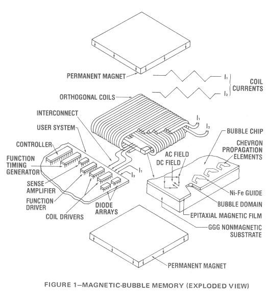
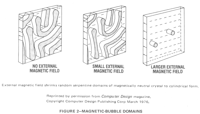
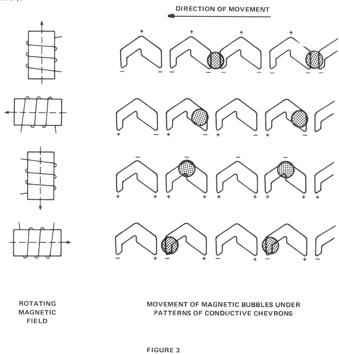
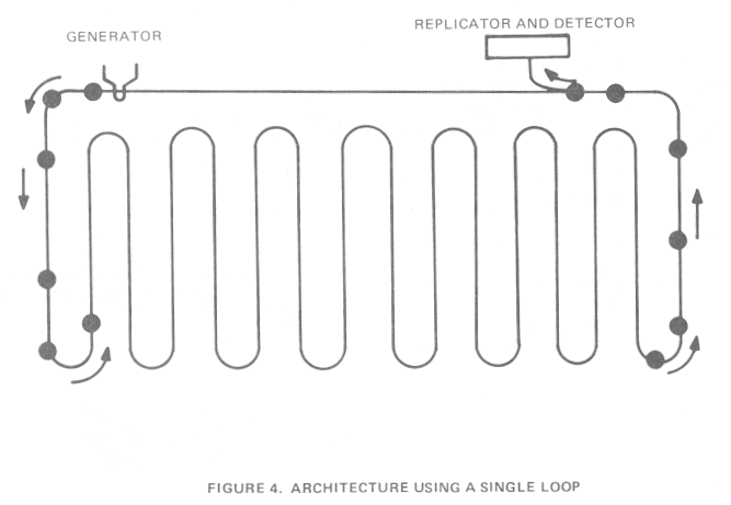
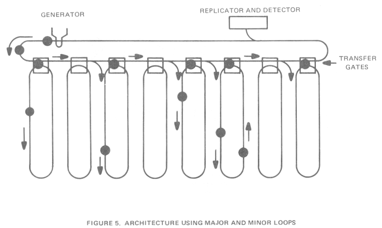
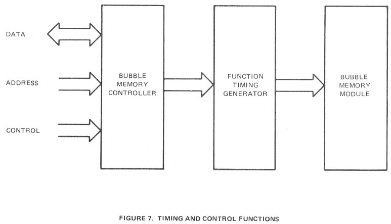
The time at which a particular
data bit is detected in the MBM may not exactly match the time at which it is
needed in the system. The sense amplifier not only increases the voltage level
of the detected data, but also provides temporary storage of the data bits in a
circuit called a D-type flip-flop. The sense amplifier receives a control input
from the function timing generator to transfer the detected data into the
internal flip-flop. In addition, the function-timing generator provides the
control signals necessary to put the existing data in a known position during a
power shut down. When the system is turned on again, the stored data can then
be accurately located and retrieved.
In a typical system the major
computing and data processing is done by a microprocessor. To provide a
convenient interface from the microprocessor to the MBM system, a custom
controller is needed for the read, write, and memory-addressing operations. The
TMS5502/TMS9916 MBM controller responds to commands from the microprocessor
system and sends control signals to the function timing generator necessary to
access a page (or pages) of data. The controller maintains page-position
information, handles serial-parallel data conversion between the bubble memory
and the microprocessor, and generates the control signals to the
function-timing generator to perform read and write operations while handling
the redundancy of the minor loops.
Advantages of bubble memories
The future growth of distributed
process systems will be greatly impacted by magnetic-bubble memories. These
microprocessor-based systems demand high-density mass storage at low cost. Magnetic-bubble
memories satisfy all of these requirements with definite advantages over the
existing magnetic storage technologies. MBM's advantages over moving-head disks
or floppy disks are low access time (the time ncessary to retrieve the desired
data), small physical size, low user entry cost, no maintenance, and higher
reliability.
The advantages of MBM's over
random-access memories (RAM's) are nonvolatility, potentially lower price per
bit, and more bits per chip. The RAM has the advantage of much better access
time, higher transfer rate, and simpler interfacing.
In summary, the main MBM
advantages are the low wnetry price versus disks for the low-end user,
nonvolatility versus semiconductor memories, and high-density storage in a
small physical space. Because magnetic bubble memories are a solid-state,
nonvolatile technology, they are ideally suited for portable applications as
well as providing memory for traditional processing systems. Industrial
applications include memory for numerical control machines and various types of
process control. Solid-state bubble memories are more reliable in harsh
environments; they are affected much less by shock, vibration, dirt, and dust
than electromechanical magnetic memories. Innovative new products include data
terminals, calculators, word processing, voice storage, and measurement
equipment.
A typical bubble memory circuit, from a
datasheet later in the publication.
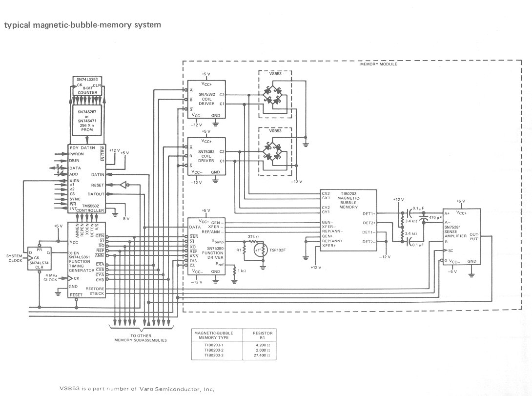
fdc